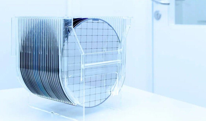
In the precision manufacturing of semiconductors, Chemical Mechanical Polishing (CMP) is a core technology for the global planarization of wafer surfaces. CMP achieves nanometer-level flatness of wafer surfaces through the synergistic effect of chemical etching and mechanical polishing. As the core medium in this process, slurry performance directly determines the surface flatness of wafers and device yield.


Chemical components in slurry mainly include oxidizing agents (most commonly H₂O₂), nano-abrasives (SiO₂, Al₂O₃, CeO₂, etc.), complexing agents, corrosion inhibitors, pH adjusters, and others. With the continuous advancement of process nodes, the application frequency of the CMP process in overall manufacturing has increased significantly, accompanied by a sharp rise in chemical consumption and extremely high purity requirements.


Accordingly, the selection of packaging and delivery materials for chemicals is critical.


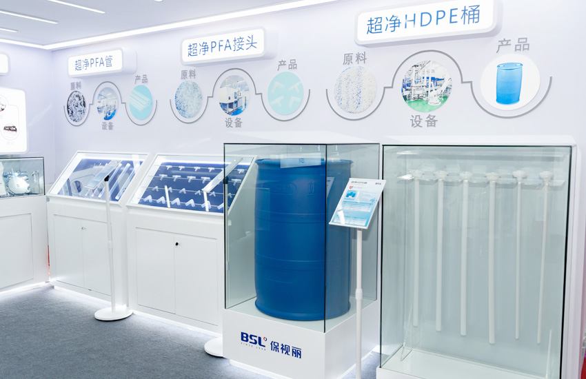
BSL (Baoshili) Ultra-Clean Solutions include high-end products such as Ultra-Clean PFA Tube, Ultra-Clean PFA Connector, Ultra-Clean HDPE Drum and Cleanroom Wiper, which effectively guarantee the purity of slurry. Except for the Cleanroom Wiper, the other three products share two key advantages: an extremely low metal ion precipitation rate and excellent chemical corrosion resistance, covering multiple links of chemical delivery, distribution, storage and transportation in the CMP process.


1. Delivery Process


Slurry delivery pipelines impose extremely high requirements on material purity and corrosion resistance. Ultra-pure PFA material is widely used in chemical delivery systems due to its outstanding chemical corrosion resistance, low ion precipitation characteristics and temperature resistance. Manufactured with ultra-pure PFA raw materials, BSL Ultra-Clean PFA Tube features reliable purity, superior stress-cracking resistance and a smooth surface, ensuring that slurry purity remains uncontaminated and flow stays stable during delivery.

In addition, slurry in the CMP process is usually acidic or alkaline, making metal impurities highly prone to chemical reactions that impair chemical performance. Through independently developed innovative processes, BSL controls the metal ion precipitation of its products to an extremely low level.


2. Distribution Process


In the CMP distribution system, slurry is transferred from storage tanks to polishing tools and distributed onto wafer surfaces. Dead spaces in chemical pipelines and connectors can easily cause nano-particles in slurry to deposit and form "dead zones", leading to particle agglomeration and eventually scratches on wafer surfaces during polishing.


With a smooth inner wall that prevents scaling and residue buildup, BSL Ultra-Clean PFA Connector achieves seamless docking and tight sealing with Ultra-Clean PFA Tube, constructing a complete, high-tightness slurry delivery system.


3. Storage Process


The core risk in slurry storage comes from residual metal catalysts in packaging materials. Oxidizing agents represented by H₂O₂ are highly oxidative. Trace amounts of transition metals (e.g., iron, copper, nickel) in HDPE drum walls can catalyze the decomposition of H₂O₂ into oxygen and water, causing container bulging or even rupture, as well as invalidation of slurry concentration.


BSL’s independently developed ultra-clean blow molding process realizes full-chain process control in production, ensuring the inner wall of the drum meets the G5 high-purity standard. For strong alkaline solutions commonly used in CMP, the Ultra-Clean HDPE Drum effectively inhibits the penetration of alkaline liquids into the polymer matrix, maintaining stable purity after long-term storage. The drum body will not swell, decompose or precipitate impurities during prolonged storage.


4. Maintenance Process


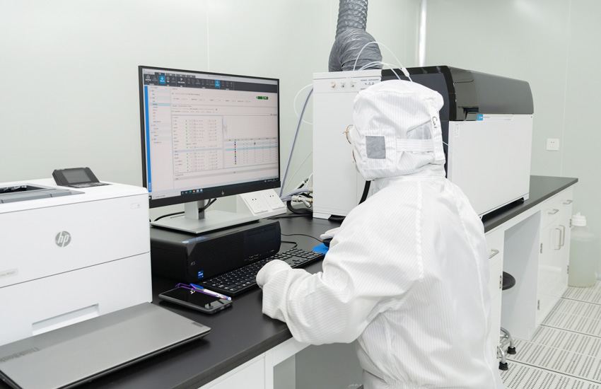
In cleanroom environments, routine cleaning and maintenance of CMP tools, pipeline systems and storage containers are essential. BSL Cleanroom Wiper delivers excellent cleaning performance with high wiping efficiency and no fiber shedding, meeting the wiping requirements for mechanical maintenance and environmental cleaning in cleanrooms.


In the CMP process, contamination at any stage — from slurry delivery pipelines and distribution connectors to storage drums and cleaning wipes — can directly impact wafer yield. Targeting the practical needs of the CMP process, BSL has built an ultra-clean solution covering the four core links of delivery, distribution, storage and cleaning maintenance. Meanwhile, as semiconductor process nodes continue to evolve, BSL will keep enhancing its independent R&D capabilities, develop more advanced consumable products for semiconductor manufacturing, and contribute to the development of the industry.

PwC recently released Semiconductors and the Future: 2026 Global Semiconductor Industry Outlook (hereinafter referred to as “the Report”). The Report systematically analyzes demand, supply, and future technology trends in the global semiconductor industry. It forecasts that the global semiconductor market size will surpass $1 trillion by 2030, with a compound annual growth rate (CAGR) of 8.6%. Driven by artificial intelligence, automotive electrification, industrial automation, and other megatrends, the semiconductor industry is undergoing profound transformation, while raising higher requirements for upstream materials, chemical delivery, and clean consumables.


As a leading domestic supplier of ultra-clean products, BSL (Baoshili) has long focused on advanced semiconductor manufacturing, committed to providing high-purity chemical delivery and clean wiping solutions for wafer fabs. This article interprets how BSL seizes industrial growth opportunities through innovative products and full-chain services, combined with the core insights of the Report.


01 Trillion-Dollar Market Drives Synchronous Upgrading of Chemical Demand


Data from the Report shows that servers & networking, automotive, and industrial applications will become the fastest-growing end markets, with projected CAGRs of 11.6%, 10.7%, and 8.8% respectively from 2024 to 2030. Expansion in these end markets will directly drive demand growth for electronic-grade chemicals (e.g., photoresists, etchants, cleaning agents, etc.), further boosting the market size of chemical packaging and delivery systems.


BSL covers the entire chemical process from packaging to delivery with four core product lines:
Ultra-Clean PFA Tube, Ultra-Clean PFA Connector, Ultra-Clean HDPE Drum, and Cleanroom Wiper.

Among them, Ultra-Clean PFA Tube meets the delivery needs of electronic-grade chemicals in key process steps such as wafer cleaning and etching. Ultra-Clean HDPE Drum — a leading domestic G5‑grade product — is used for the storage and transportation of high-purity chemicals, with its 200L model now under customer validation, providing pure packaging support for high-end processes. With the continuous expansion of semiconductor capacity, BSL’s product portfolio is precisely positioned in the incremental market.


02 Technological Iteration: Purity and Delivery Precision Become Critical


The Report points out that semiconductor technology is evolving toward advanced processes (below 7nm), wide-bandgap semiconductor materials (SiC/GaN), 3D packaging, and chiplet architectures. These technologies impose extremely stringent requirements on chemical purity, delivery stability, and cleanliness — any micron-level particles or extractables can reduce wafer yield and increase manufacturing costs.


BSL’s Ultra-Clean PFA Tube meets the strict demands of advanced processes, achieving ppt-level metal extractable control during delivery to ensure stable chemical quality. Ultra-Clean PFA Connectors work with Ultra-Clean PFA Tubes to build a highly sealed delivery system, effectively preventing secondary contamination.


03 Supply Chain Resilience Grows Prominent; Independent Technologies Consolidate Security Foundation


Against the backdrop of geopolitics and regionalized production, supply chain resilience and security have become core concerns for semiconductor enterprises. The Report notes that countries are increasing investment in local manufacturing. Even chemical packaging materials — a segment in the upstream supply chain of the semiconductor industry — are facing higher requirements in terms of safety, timeliness, and compliance.


BSL’s technological core stems from in-depth control over material properties, production processes, and manufacturing environments. From environmental control in dust-free workshops to precision testing before packaging, BSL establishes strict purity standards at every step, ensuring extremely low extractables and zero secondary contamination when products contact high-purity chemicals. Amid the ongoing supply chain restructuring, technological independence has become a key factor for more wafer fabs and chemical material suppliers to choose BSL.


04 Forward-looking Layout: Embracing Future Application Scenarios


The Report analyzes and forecasts innovative semiconductor-related technologies beyond 2030, including artificial intelligence, quantum computing, brain-computer interfaces, humanoid robots, and more. These cutting-edge fields will drive demand for specialty chemicals, such as material delivery in cryogenic environments, ultra-high-precision micro-dosing, and biocompatible packaging.


BSL is not resting on its existing product portfolio, but continuing to invest in R&D to develop chemical protection solutions adapted for next-generation semiconductor technologies. As the global semiconductor market moves toward a trillion-dollar scale, BSL will further deepen technological innovation, and work with industry partners to shape the future of clean semiconductor manufacturing with reliable products and services.

keyboard_arrow_up