The rapid development of high-end industries including new energy vehicles, photovoltaic energy storage and consumer electronics is driving wide bandgap semiconductor materials represented by Silicon Carbide (SiC) and Gallium Nitride (GaN) to gradually replace traditional silicon-based materials. Featuring excellent properties such as high breakdown electric field and high thermal conductivity, wide bandgap semiconductor materials have become the core pillar for improving device performance.


The market for wide bandgap semiconductor materials has maintained robust growth in recent years. The global market size of SiC power components is projected to reach 4.96 billion US dollars in 2026 and rise to 8.95 billion US dollars by 2032. Meanwhile, the global GaN power device market is expected to hit 920 million US dollars in 2026, representing a year-on-year growth of 58%.



01 Trace Impurities Bring Fatal Hazards to Devices

The large-scale adoption of wide bandgap semiconductor materials has set new stringent requirements for the purity of electronic chemicals.

Although SiC and GaN possess extremely high chemical stability and are barely reactive with common acids, alkalis and organic solvents, metallic impurities (e.g. Fe, Cu, Ni), particulates and organic contaminants introduced during production cannot be easily dissolved or removed by subsequent cleaning processes, unlike those on silicon surfaces. Such contaminants adhere to the inert material surface via physical adsorption and chemical bonding, forming stubborn contamination layers that directly lead to performance degradation or even scrapped devices. For this reason, chemicals used in wide bandgap semiconductor manufacturing processes must meet a purity standard of 6N grade or above.

02 How to Maintain the Ultimate Purity of Chemicals

Throughout the entire delivery process of ultra-high-purity chemicals from storage to process tools, the cleanliness of transfer tubing is one of the decisive factors. The rigorous process requirements for tubing in wide bandgap semiconductor manufacturing are raising the bar for tubing performance standards.

Chemical transfer tubing for such applications must deliver core capabilities including extreme chemical inertness, ultra-low ion leaching (with metallic ions controlled at the ppt level), minimal particulate shedding and long-term stable structural performance. Supported by sophisticated manufacturing techniques, BSL Ultra-Clean PFA Tube boasts outstanding corrosion resistance, high cleanliness and excellent compatibility with ultra-pure fluids, fully catering to the demanding requirements of wide bandgap semiconductor processes.

03 Ultra-Clean PFA Tube Perfectly Matches Advanced Material Processes

BSL Ultra-Clean PFA Tube is manufactured with imported ultra-pure PFA raw materials to guarantee cleanliness from the source. The tube wall features superior chemical resistance to electronic chemicals, with metallic ion leaching kept at the ppt level and particulate release complying with the SEMI F57 industry standard for semiconductors. All these properties are highly aligned with the chemical purity requirements of wide bandgap semiconductor processes.
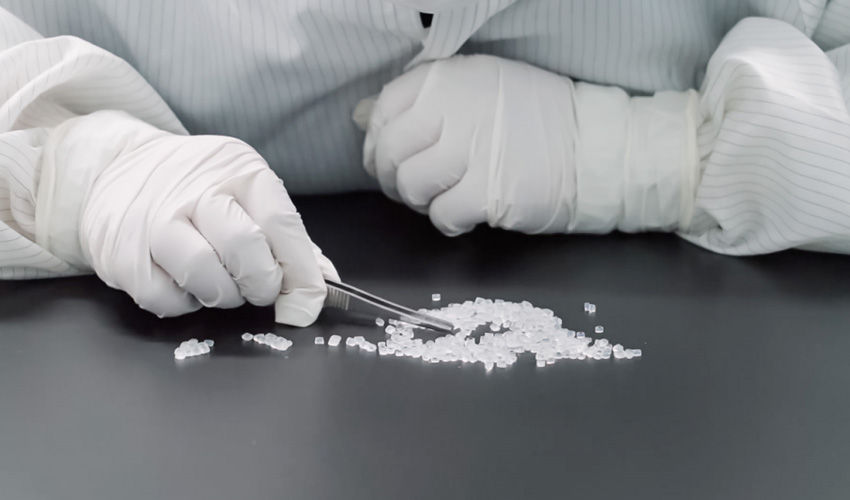


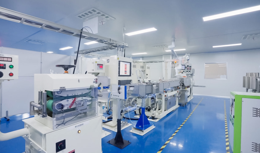
On the production side, BSL has established a comprehensive process control system. The entire workflow including extrusion, assembly and packaging is completed inside cleanrooms to eliminate external contamination. Adopting precision extrusion molding technology, the tubing is made with a smooth inner wall free of dead corners and residual contaminants, which effectively reduces particulate generation from the physical structure.


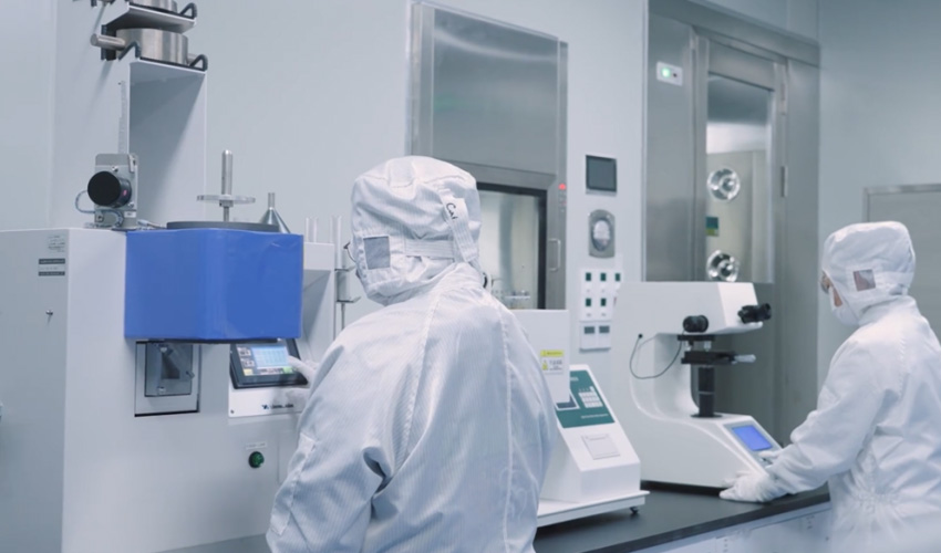
On the testing side, BSL runs a Class 100 laboratory. Every product batch undergoes full-scale tests covering physical properties, chemical properties and cleanliness. Real-time on-line inspection is implemented for tube wall thickness and outer diameter during production to ensure consistent dimensional stability.


The application of wide bandgap semiconductor materials has continued to expand in recent years. SiC and GaN are being deployed in an increasing number of high-value scenarios, ranging from main drive inverters and photovoltaic inverters to fast charging power supplies and power supply systems for data centers. The year 2026 is poised to become a critical window for breakthroughs in the wide bandgap semiconductor device market, followed by an industry-wide capacity expansion boom.

As purity requirements and packaging standards for electronic chemicals keep upgrading, the quality of Ultra-Clean PFA Tube — a core component in chemical transfer — is directly linked to the yield rate and performance of chip manufacturing. BSL Ultra-Clean PFA Tube is designed to preserve chemical purity and prevent contamination during transportation, making it an indispensable fundamental safeguard for the manufacturing processes of wide bandgap semiconductor materials.
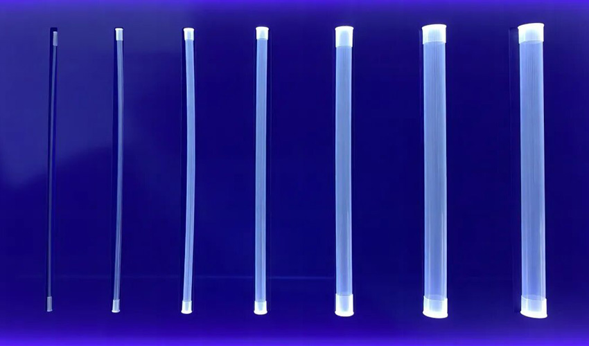
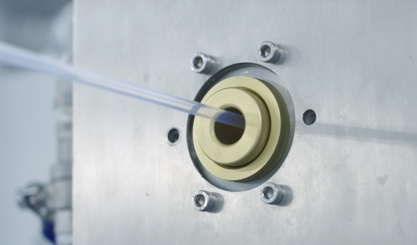

Boasting excellent chemical inertness, ultra-low metal ion leaching, superior inner wall smoothness and outstanding stability over a wide temperature range, Ultra-Clean PFA Tube serves as an essential core pipeline component for semiconductor photoresist transfer systems.


ultra-clean PFA Tube


As chip manufacturing processes evolve toward more advanced nodes, fabrication fabs have raised stricter standards for the purity and particle control of photoresist delivery pipelines. As a vital fluid passage connecting storage tanks, pumps, valves and other components, Ultra-Clean PFA Tube must withstand long-term corrosion from strong organic solvents in photoresists. Meanwhile, it is required to deliver ultra-low metal ion leaching and superior particle control performance, so as to minimize photoresist contamination and ensure the yield of products manufactured by advanced processes.

For a long time, the domestic market for semiconductor-grade Ultra-Clean PFA Tube has been highly dependent on imports. Particularly for the production of advanced logic and memory chips, high-end products are still dominated by a small number of international manufacturers. Faced with technical bottlenecks in core fluid pipeline materials for semiconductors, BSL has continuously made breakthroughs in key processes including precision extrusion molding of high-purity PFA, steadily improved the control capability of metal leaching, and upgraded full-process clean manufacturing technologies. In addition, BSL is accelerating product verification and on-site application at mainstream fabs and semiconductor equipment suppliers. Our product portfolio features high batch consistency, superior chemical resistance and ultra-high purity, fully meeting the rigorous requirements of photoresist transfer systems for advanced processes. It provides solid support for the independent controllability and sustainable development of key semiconductor consumables.

01 Chemical Resistance


BSL adopts high-purity PFA raw materials. Innovative processes improve the density and uniform molecular structure of the tubes, reduce micropores and weld defects, and effectively block penetration channels for corrosive media, which greatly enhances the overall corrosion resistance and anti-swelling performance. When in long-term contact with common organic solvents for photoresists (such as PGMEA and Cyclohexanone), as well as chemicals widely used in semiconductor wet processes including sulfuric acid and hydrofluoric acid, the tubes show no swelling, cracking or mass loss, delivering excellent chemical resistance.

Test results show that after 168 hours of immersion in 37% hydrochloric acid at 85℃, BSL Ultra-Clean PFA Tube has no obvious changes in appearance and dimensions, and the total leachables remain stable. Its overall chemical resistance has reached the world’s advanced level.

02 Low Metal Ion Leaching


Manufactured with high-precision production equipment, BSL Ultra-Clean PFA Tube maintains ultra-high purity. In compliance with the Group Standard for Semiconductor-Grade Perfluoroalkoxy (PFA) Tubes (hereinafter referred to as the Standard), the leaching levels of metal ions such as aluminum, calcium, chromium, iron and sodium are all controlled below the limits specified in the Standard. Especially for critical impurities including sodium, iron and calcium, our product delivers performance equivalent to or even better than international competing products, ensuring fluid purity from pipelines to wafers throughout the whole process.

03 Low TOC and Particulate Leaching

The tubes undergo ultrasonic cleaning and multi-stage ultrapure water flushing, which drastically reduces organic residues and loose particulates on the inner wall. The Standard stipulates that the total organic carbon (TOC) content shall not exceed 2000 μg/m², while the actual measured TOC value of BSL products is controlled within 60% of the standard limit.

In addition, particulate leaching fully complies with SEMI Standards. In particle-sensitive photolithography processes such as photoresist coating and development, particle detachment from the tube inner wall is kept to a minimum, avoiding wafer surface scratches and short-circuit defects.

04 Smooth Inner Surface

Adopting high-precision extrusion dies and stable process parameters, the average surface roughness (Ra) of the tube inner wall of BSL products is steadily controlled at ≤0.25 μm. Atomic Force Microscope (AFM) tests verify that the inner wall is smooth and free of microcracks. This effectively suppresses fluid turbulence and reduces particle adhesion and chemical residue accumulation.

Independently developed BSL Ultra-Clean PFA series products fully satisfy the extreme demands of advanced semiconductor processes for photoresist transfer. They are applicable to harsh working scenarios requiring high cleanliness, strong corrosion resistance and high precision, ensuring stable operation of fluid transfer systems and protecting manufacturing yield.


keyboard_arrow_up